A team of international researchers, including a 2DFERROPLEX team member, have developed a novel multifunctional ferroelectric field-effect transistor using a new split-gate architecture that can switch between different logic and computing operations while automatically erasing sensitive data after a short period (~100 s), offering a new solution for secure and energy-efficient hardware suited for “Zero-Trust” environments.
The rapid expansion of artificial intelligence and the Internet of Things (IoT) needs faster, more adaptable, and more energy-efficient computing and memory technologies. Conventional semiconductor devices often struggle to meet these requirements. Multifunctional devices that can integrate memory and logic within a compact architecture while maintaining robust security against data theft are needed. Ferroelectric technology has emerged as a solution to address these challenges.
Now, an international team of researchers, including 2DFERROPLEX team member Jean-François Dayen from the IPCMS – Université de Strasbourg and Dr. Ankita Ram, in collaboration with researchers from the École Centrale de Lyon, University of Nebraska, Université Paris-Saclay, and National Institute for Materials Science (Japan), reports in Advanced Electronic Materials the development of an α-In2Se3 ferroelectric semiconductor field-effect transistor (FeS-FET) with a split-gate architecture. The new device leverages some of the semiconductor and ferroelectric properties of the van der Waals material α-In2Se3 to perform volatile NAND logic, reconfigurable Fe-NAND/Fe-NOR operations, and multilevel analog computing. The device also has a short retention time, which enables the self-erase of programmed states.
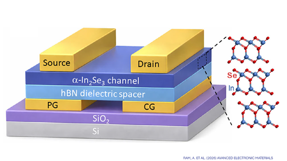
The split-gate architecture
The split-gate design is at the heart of this new transistor, a small device that can amplify or switch electrical signals and which is a central component of modern chips. This architecture utilizes two independent gate electrodes to tune and control ferroelectric and semiconducting states in two consecutive segments of the channel.
Unlike conventional transistors, this device operates in a high Equivalent Oxide Thickness (EOT) regime, where the electric field is localized at the bottom layers of the α-In2Se3 film. This allows for the simultaneous manipulation of ferroelectric bound charges and the redistribution of mobile carriers within the α-In2Se3 channel, resulting in distinct conductance states that can be programmed and stored.
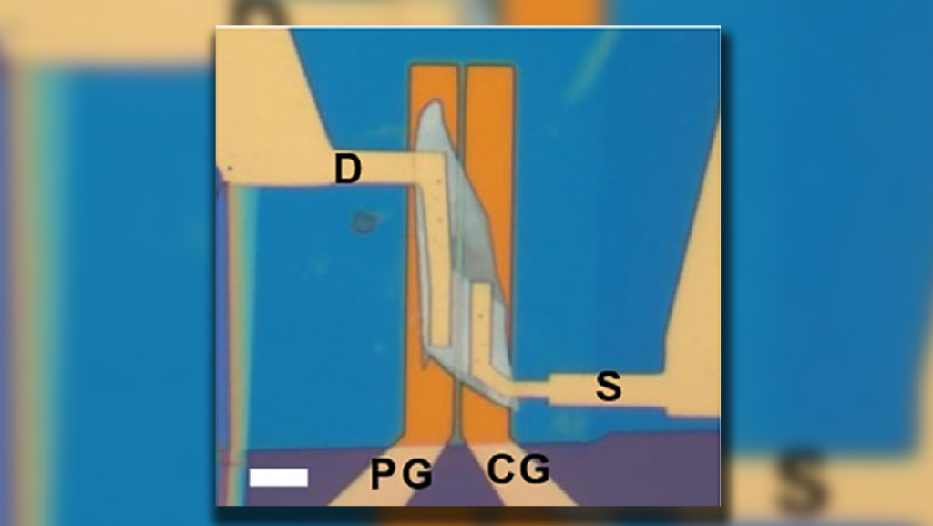
To build the new transistor, the team fabricated a van der Waals heterostructure by exfoliating ultra-thin flakes of hexagonal boron nitride (hBN) and α-In2Se3 from bulk crystals. These flakes, just a few atoms thick, were then transferred onto pre-patterned titanium/gold (Ti/Au) split-gates on a silicon substrate. The researchers characterized the fabricated samples using micro-Raman spectroscopy to confirm the material’s phase and piezoresponse force microscopy (PFM) to verify its ferroelectric switching capabilities.
“We decided to use α-In2Se3 because it combines semiconductivity and ferroelectricity, allowing at the same time to compute and store information,” explained Jean-François Dayen, leading author of the study. “We have seen that these unique properties allow for developing reconfigurable devices, a sort of multifunctional Swiss Army knife for information processing, together with presenting original remanency properties suitable for zero-trust security environments.”
A new solution for “Zero-Trust” environments
The device is designed to address the paradigm of Zero-Trust (ZT) security architectures. In a Zero-Trust environment, no user or device is implicitly trusted, and access to resources must be continuously verified. That is why the researchers focused on minimizing the “persistence” of sensitive information, exploiting the short retention time of ferroelectric states.
In this FeS-FET, sensitive data, such as a security key, is stored in the ferroelectric polarization of the channel, a state that is only temporary and that can be flipped by an external applied voltage. In the tests, the device showed a “balanced” retention time of approximately 102 seconds, after which the information disappeared. This “self-erasing” feature ensures that the window of time in which data could be accessed by an attacker is small, providing a defense against attacks.
“This newly developed split-gate FeS-FET provides a proof of concept for a compact and energy-efficient architecture, unifying logic, memory, reconfigurability, and security within a single framework,” said Jean-François Dayen. “We have demonstrated that van der Waals ferroelectric semiconductors, like α-In2Se3, are a promising platform for secure and versatile nanoelectronics and can be a key piece for future beyond-CMOS technologies,” concluded Dayen.
Original article
A. Ram, C. Marchand, S. B. Masood, et al. Logic Functionality and Circuit Design of α-In2Se3 -Based Split-Gate Ferroelectric Field-Effect Transistor for Zero-Trust Applications. Adv. Electron. Mater. (2026). DOI: https://doi.org/10.1002/aelm.202500871